LASER DRILLING AND CUTTING
From microvias and cavity formation to coverlay patterning, PPI has the application experience to help you improve productivity.
The Applications Lab team at PPI have a wealth of experience in laser processing. They will help you choose the right laser for your application, whether HDI microvia drilling, or kiss-cutting polyimide coverlay.
For polyimide or other non-reinforced dielectrics, the UV laser alone may provide your solution. With the glass-reinforced dielectrics of rigid boards, the hybrid version with both laser sources is the best choice. The high peak power pulses of the CO2 laser can also be used for drilling of small vias directly through both the top Cu and dielectric. In general, the CO2 laser is appropriate for high speed drilling, cutting and skiving of dielectrics, while the UV laser is able to machine copper and provide higher process quality in many dielectrics.
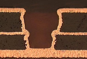
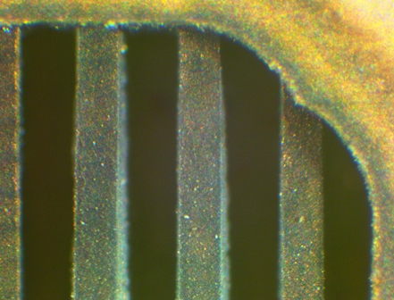
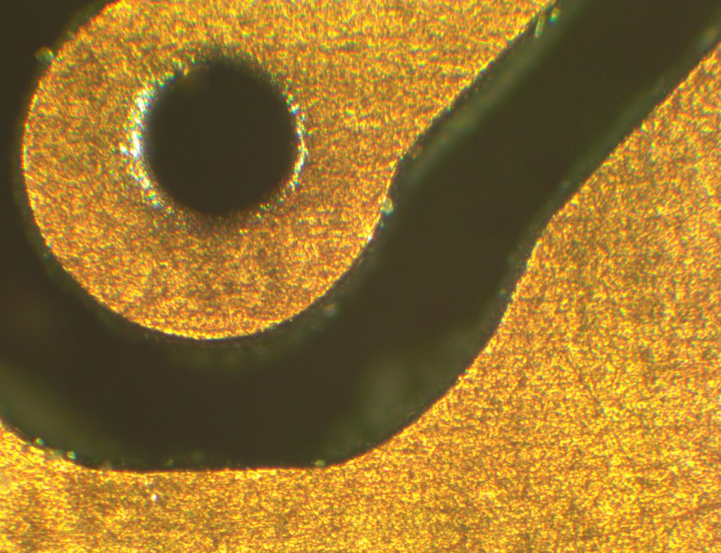
HDI Micro Vias
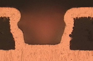
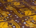
Automatically drill not only single layer vias but also double layer (stepped) blind vias and through holes using a combination of UV and CO2 lasers.
Cavity Formation
Machine through top copper with a UV laser and then the dielectric without damage to buried tracks or pads. A final process step with weak UV cleans the lower Cu layer.
Green Tape
Green ceramic tape is easily drilled, cut or depth-machined with either the UV or CO2 laser.
CO2 Direct Drilling
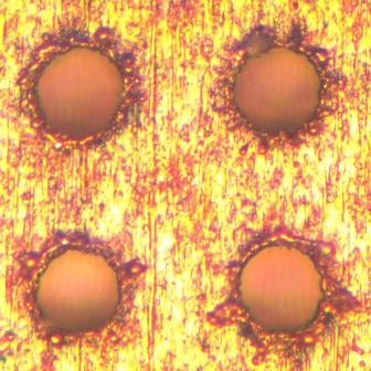
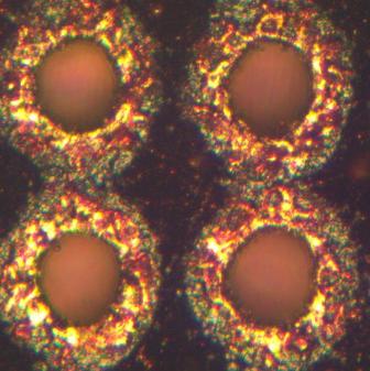
Drill directly into thin Cu with CO2 down to a 40 μm diameter with or without black oxide.
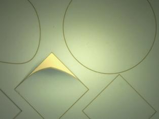
Flex Circuit Processing
Usually performed on polyimide and copper. Typical processes include drilling, cutting and skiving.
Structure Copper
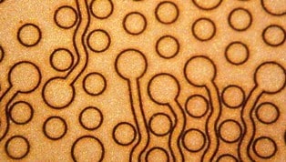
Directly structure Cu (including thin) using the UV beam with little damage to underlying materials.
Coverlay
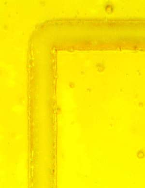
Kiss cuts through polyimide / adhesive coverlay.
Solder Mask Repair
Panels with mistakes in solder mask can be salvaged by solder mask removal with either the CO2 or UV laser.
